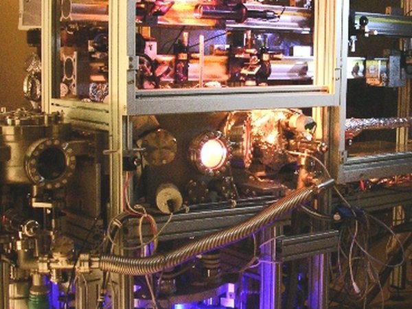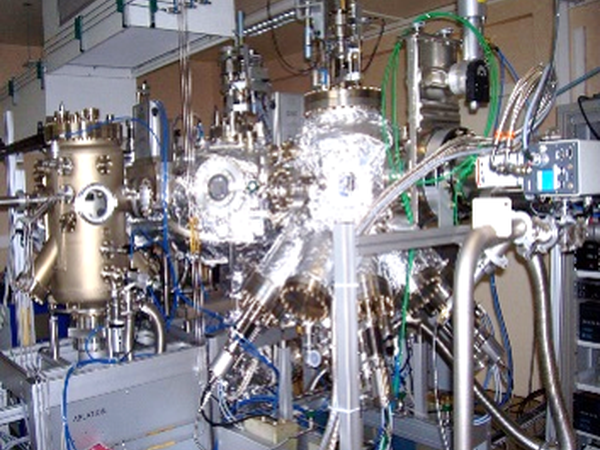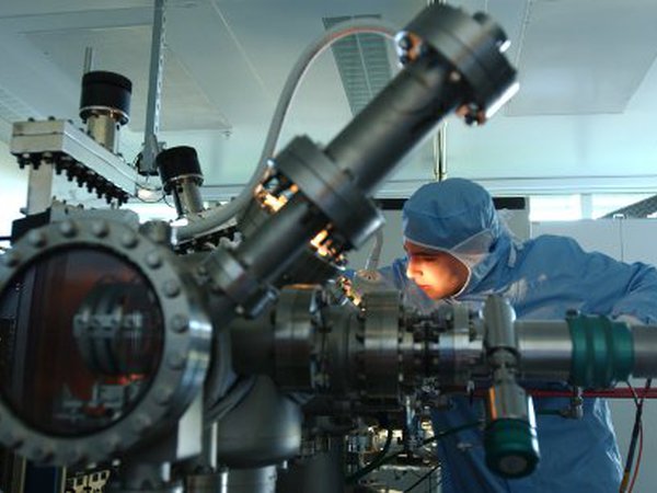
MBE FOR III-V SEMICONDUCTORS
Members: Antonella Cavanna (IR), Martina Morassi (IE), Laurent Travers (IE)
MBE FOR III-V SEMICONDUCTORS
Members: Antonella Cavanna (IR), Martina Morassi (IE), Laurent Travers (IE)
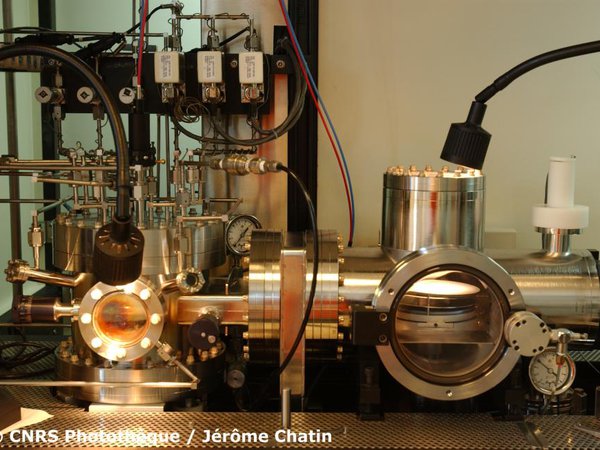
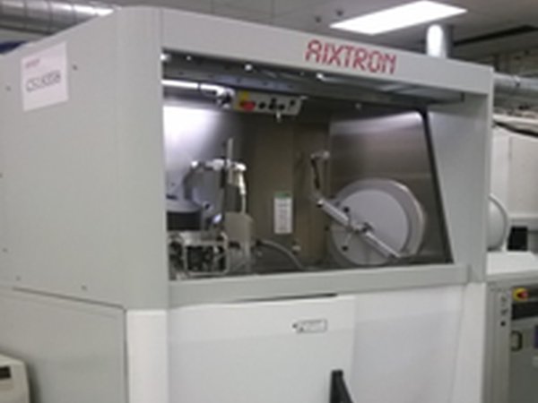
MOVPE & UHV CVD FOR III-V & SiGeSn MATERIALS
Members: Gregoire Beaudoin (IR), Géraldine Hallais (IR)
Key Figures
Platform manager
News
March 2024: reception MO-MBE to growth thick epitaxial oxide films
January 2024: welcome toDavide Cammilleri who joined us for implementing equipment for the development of oxide thin films.
April 2023: JUICE Mission: achievement of more than 10 years of collaboration between C2N researchers & engineers and LERMA to develop Teraherzt state-of-the-art heterodyne components embedded in the Jupiter probe. The fisrt material step has been developped on material growth facilties (POEM) and nanoprocessing on PIMENT Facilities, Phynano group and LERMA engineers.
May 2023: conference ENRIS at C2N-Palaiseau
September 2022: Plaquette Centrale du C2N version numérique.pdf
February 2022: reception of new ECV Profilometer Equipment
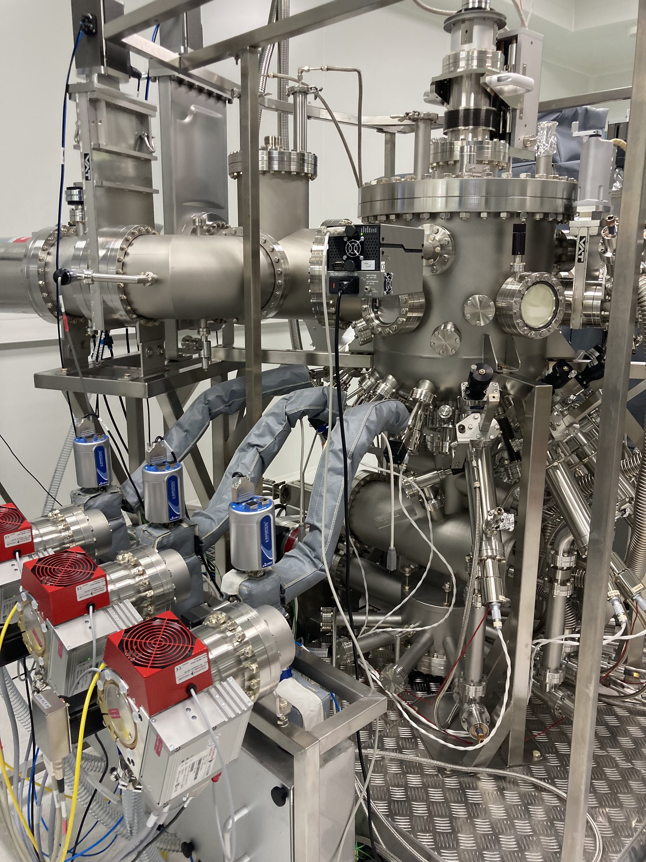
January 2021: reception of the new III-V MOVCD
March 2020: COVID-19 Lock-down
February 2020: Fourth Edition Nano-TN 2020
February 2020: reception of new TRT MBE
November 2019: Rencontre Thématique RENATECH "Croissance cristalline" at LTM-Grenoble/C2N
This pool of expertise is part of the Department of Materials. It supplies samples for national and international collaborations or projects. In particular, epitaxy is strongly involved in device activities including lasers and detectors for telecommunications, all-optical devices, transistors. Other important topics where epitaxy has a significant role are: spintronic, 2D electron gas, physics of nanostructures, photonic crystals, microcavities, functional oxides, hybrid materials...