Contact: Noëlle Gogneau
With the amount of connected objects constantly on a rise, it becomes critical to deal with the associated increase in energy consumption. Their energetic autonomy is today a key worldwide challenge, particularly for electronic systems operating in an environment with restricted, or even absent, electrical grid infrastructure.
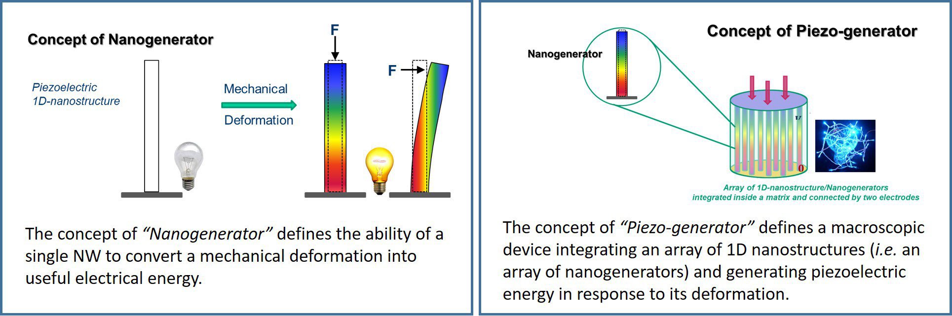
Energy harvesting, i.e. direct conversion of the ambient energy found from the vicinity of the device into usable electrical energy without any external voltage source, appears as a promising approach to power wireless micro-devices. Among the alternative sustainable energy resources, the mechanical deformations and vibrations present the advantages to be ubiquitous and permanently available. These energies may have various origins such as vibrations, friction, body movements or sound… Piezoelectric generators integrating 1D-nanostructures, such as nanowires (NWs), have emerged these last years as a powerful solution to harvest these mechanical deformations and vibrations and supply micro-devices such as micro-sensors or medical implants.
III-nitride Nanowires have started to be explored for developing piezo-generator devices thanks to their high piezoelectric coefficients and their strong piezo-generation response.
We aim to develop ultra-compact and high-efficient piezo-generators integrating vertical array of III-Nitride NWs for powering micro-devices. Our approach is based a multi scale analyses going from the NW synthesis to the fabrication and testing of generators, while passing by the characterization of the piezoelectric properties of unique NWs and the investigation of the piezo-mechanisms in play.
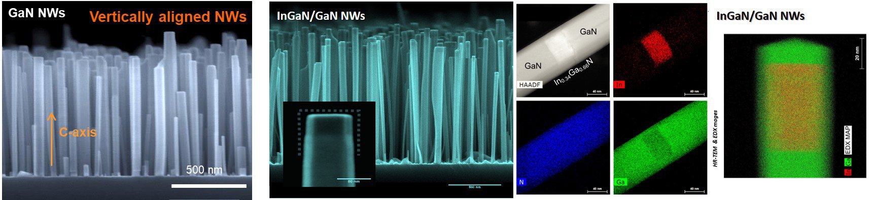
Our III-N NWs
Self-assembled III-N NWs are grown by Plasma-Assisted Molecular Beam Epitaxy on Si(111) substrate. Prior to the growth of GaN NWs, a 2.5 nm-thick AlN buffer layer is deposited. This AlN underlayer allows a better control of the NW nucleation, density and orientation and prevents the formation of the insulating SiN layer between the GaN NWs and the Si(111) substrate, which annihilates the piezoelectric generation.
Our GaN NWs are vertically aligned with hexagonal cross-section delimited by {10-10} planes and they are characterized by a N-polar surface (N-polarity).
Piezoelectric properties of III-N NWs
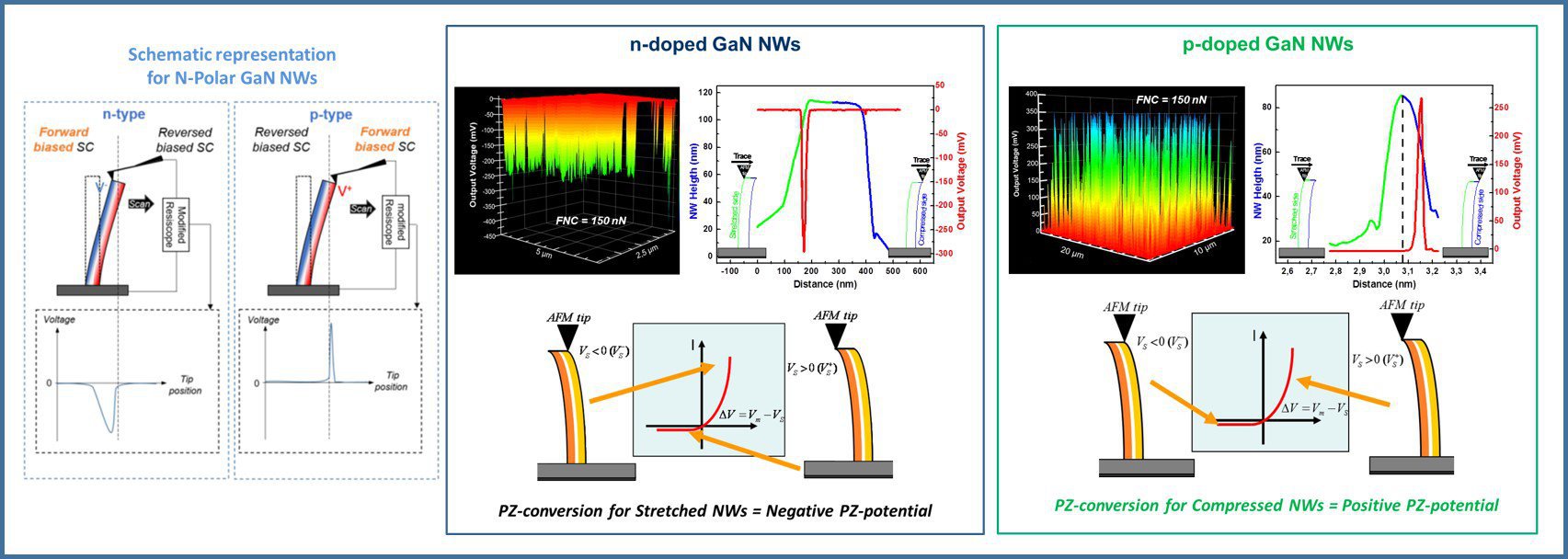
We investigate the piezoelectric properties of single GaN NWs by atomic force microscope (AFM) in vertical configuration equipped with a modified Resiscope module allowing real-time electrical measurements (Collaboration with the GEEPs Lab from CNRS, CentraleSupelec, Paris-Saclay Univ. & Paris-Sorbonne Univ.).
Vertical Scanning Configuration: Allows to simultaneous record Topographic and Electric signals in the case of a laterally bended NW.
Following this experimental configuration, we have demonstrated the high potential of Ga(In)N NWs to convert a mechanical deformation into an electrical energy. In terms of output voltage:
GaN nanowires for piezoelectric generators – Phys. Status Solidi RRL 2014
High Piezoelectric Conversion Properties of Axial InGaN/GaN Nanowires, Nanomaterials 2018
Mechanical-electrical conversion mechanisms in III-N NWs
We demonstrate the strong relationship between the structural and electrical (doping) properties of the GaN NWs and the establishment of the piezo-electric potential inside the nanostructures when they are submitted to a deformation. The harvesting of the piezo-generated energy through a Schottky contact is depending on the establishment of the piezo-electric potential inside the nanostructures.
Energy harvesting efficiency in GaN nanowire: the critical influence of the Schottky nanocontact
The performances of 1D-nanostructure based nanogenerators are governed by the ability of nanostructures to efficiently convert mechanical deformation into electrical energy, and by the efficiency with which this piezo-generated energy is harvested. We have demonstrated that the harvesting efficiency of piezoelectric energy generated by Ga(In)N nanowires is strongly affected by Schottky nanocontact properties at interface with electrode. Under nanometer scale conditions, the contact is governed by its nanometer size. The contribution of the tunneling emission greatly increases, becoming dominant, and thus gives rise to an improved conductance per unit area, leading thus to a more efficient harvesting.
The design of the Piezo-generator is based on GaN NWs having high piezoelectric response and takes into account of the relationship existing between the material properties and the piezoelectric generation mechanism.
We demonstrate the first piezo-generator integrating vertical array of p-doped GaN NWs operating under compressive strain. The maximum power density delivers by the generators can reach several tens of mW/cm3. This value states the new state of the art for nitride piezo-generators and opens the way for powering electronic devices, such as medical implants.
The flexibility is the key point enabling the conformal integration of generators on different objects with arbitrary shape. It is thus crucial to integrate the piezoelectric NWs onto soft flexible substrates.


People
Collaborations
C2N
Dr. M. Tchernycheva, Dr. F. Julien from Photonic Dept.
Prof. E. Lefeuvre from Microsystems and Nanobiofluidics Dept.
France
GeePs: Dr. P. Chrétien, Dr. F. Houzé
SPMS : Prof. B. Dkhil, Prof. P-E. Janolin
MSSMAT: Prof. D. Aubry, Prof. A-L. Hamon, Dr. J. Bai
GEMAC: Dr. V. Sallet
LSI: Dr. M-C. Clochard, Prof. J-E. Wegrowe
IEMN: Prof. E. Dogheche
INAC/CEA-Grenoble: Dr. J. Eymery
GPM: Dr. L. Rigutti
International
KAIST , South Korea: Prof. Y-H CHO
CNU, South Korea: Prof. S-W RYU
CINTRA, Singapore: Prof. P. Coquet, Prof. Wang Hong, Dr. M. D. Birowosuto
CSIR-NIIST, India: Dr. S. Das
Connections
GDR « Pulse » - Axis “Epitaxial systems properties and applications”
National Research Group PULSE dedicated to epitaxy of semiconductor systems with an in-depth understanding of the growth mechanisms and the development of innovative approach in order to allow major progress
Fundings


