Contact: Jean-Christophe HARMAND
In 2016, C2N demonstrated that it is possible to epitaxially grow GaN nanowires on graphene by MBE [1]. The epitaxial relationship is illustrated in Fig. 1. Our work showed that it was neither a van der Waals epitaxy (the latter having been obtained by MOVPE growth [2]), nor a “remote epitaxy” mechanism involving an underlying crystalline substrate [3] (in our case, graphene was transferred onto a thick amorphous silica layer).
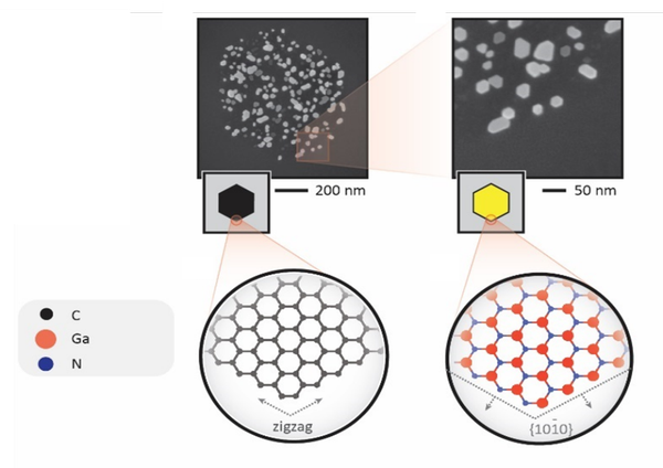
Figure 1: Selective epitaxy of GaN nanowires on a single-crystal graphene domain of hexagonal shape, transferred onto SiO2. All the nanowires have the same basal orientation. Their {10-10} planes are parallel to the zigzag directions of the graphene domain.
Three observations indicate that chemical bonds establish between the graphene sheet and the GaN nanocrystals:
(i) at the nucleation stage, GaN was found to be strained [4];
(ii) XPS measurements revealed the presence of C-N bonds, with N atoms occupying pyridine sites [5];
(iii) nanowire attachment on graphene was found to resist mechanically to a force exerted by an AFM tip and high enough to overcome van der Waals forces [6].
A long incubation time precedes the establishment of these first chemical bonds and corresponds to a modification of the graphene lattice to make them possible. The nanowires are nitrogen polar. At an adequate temperature, growth is perfectly selective between graphene and silica (Fig. 1). This enables us to fabricate organised nanowire arrays with a controlled pitch by patterning graphene into dots by electron lithography (Fig. 2). Our aim is to obtain one and only one nanowire per graphene dot.
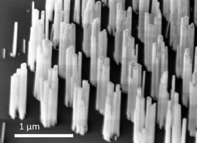
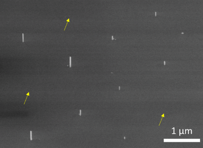
Figure 2: Organised arrays of GaN nanowires on patterned graphene. On the left image, the pattern consists of 200-nm-diameter graphene discs: several nanowires have grown on each site. On the right image, the pattern consists of 30-nm-diameter graphene dots: a single nanowire has nucleated on each dot. However, at certain sites indicated by the arrows, either the graphene dot has removed or no nanowires have nucleated on it.
The next step is to use these nanowires as seeds for lateral overgrowth which is performed by our collaborators: PHELIQS Université Grenoble Alpes/CEA by using MOVPE, and Institut Pascal, Université Clermont Auvergne, using HVPE. With both epitaxy techniques, lateral regrowth have been successful. We have obtained a-few-µm-wide GaN micro-domains (Fig. 3) which can be completely free of extensive defects (Fig. 4). This process is still being optimized.
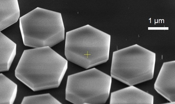
Figure 3: Array of GaN micro-domains (about 2 µm wide) obtained by lateral HVPE overgrowth on GaN nanowires on graphene. The substrate is SiO2. The graphene is patterned by electron beam lithography. The orientation of the domains follows that of the grains of polycrystalline graphene initially deposited on SiO2.
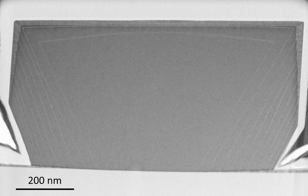
Figure 4: TEM cross-section of a GaN micro-domain obtained by MOVPE lateral overgrowth on a GaN nanowire grown by MBE on graphene. AlN markers are introduced to monitor the lateral growth process. The domain is free of extended defects.
These micro-domains will be used as micro-substrates to grow active device structures on their upper surface. Our approach combines several advantages:
• It eliminates the need of monocrystalline bulk substrates.
• If lateral growth does indeed take place on a single seed and if there is no coalescence of several domains, these GaN micro-substrates do not contain an extended defect.
• The GaN domains are weakly bonded to the SiO2 support and can therefore be easily detached for transfer to a flexible support, for example.
• The concept could be extended to Ga1-xInxN micro-substrates for red LEDs.
[1] V. Kumaresan et al., Epitaxy of GaN nanowires on graphene, Nano Lett. 2016, 16, 4895−4902. [DOI]
[2] T. Journot et al., Remote epitaxy using graphene enables growth of stress-free GaN, Nanotechnology 2019, 30, 505603 [DOI]
[3] Y. Kim et al., Remote epitaxy through graphene enables two-dimensional material-based layer transfer, Nature 2017, 544, 340−343 [DOI]
[4] C. Barbier et al., In situ X-ray diffraction study of GaN nucleation on transferred graphene, Cryst. Growth Des. 2020, 20, 4013−4019 [DOI]
[5] C. Barbier et al., What triggers epitaxial growth of GaN on graphene? Cryst. Growth Des. 2023 23 (9), 6517-6525 [DOI]
[6] M. Morassi, Cryst. Growth Des. 2020, 20, 2, 552–559 [DOI]
People
Collaborations
Institut Pascal, Université Clermont Auvergne, Clermont-Ferrand
PHELIQS, Université Grenoble Alpes, CEA, Grenoble
Fundings
